

-
Company Introduction
-
Business Field
-
Product Introduction
-
Recruitment
-
Community
R&D
R&D
Functional Coating Materials
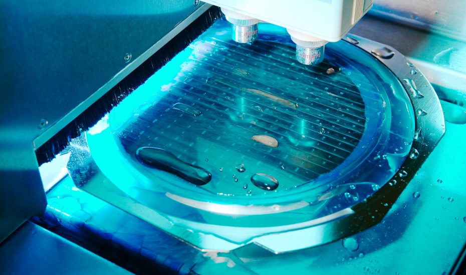
Functional coating materials are materials and solutions that temporarily protect the device surface from various foreign substances generated during the semiconductor/display manufacturing process and can be easily removed with water or exclusive stripping solution after the necessary process is completed. MTI develops and supplies various coating material products according to customer requests based on coating material synthesis, formulation, and additive application technology.
- Functional coating agent to protect material surface from B/G tape residue
- Functional coating agent to protect the interface from foreign substances
- Functional coating agent to generated during the post-process of the image sensor
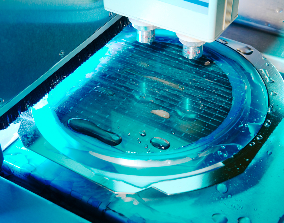
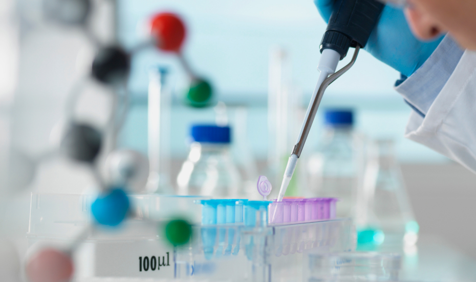
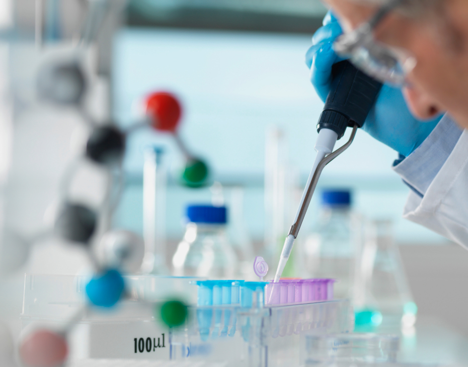
Functional Cleaner
Functional cleaners are intended to remove various organic substances and foreign substances generated during the mobile/semiconductor/display manufacturing process. The role of cleaning is becoming more important as the types and shapes of foreign substances diversify as devices become increasingly fine/layered. MTI is developing various types of detergents (acid, alkali, neutral surfactant, etc.) depending on the type of foreign matter generated during the mobile/semiconductor/display manufacturing process.
- Glass cleaner for mobile (for normal process, for rework)
- Wafer cleaner (for package sawing, blade dicing)
- OLED Metal Mask Cleaner (Metal Cleaner)
- Various cured ink cleaners
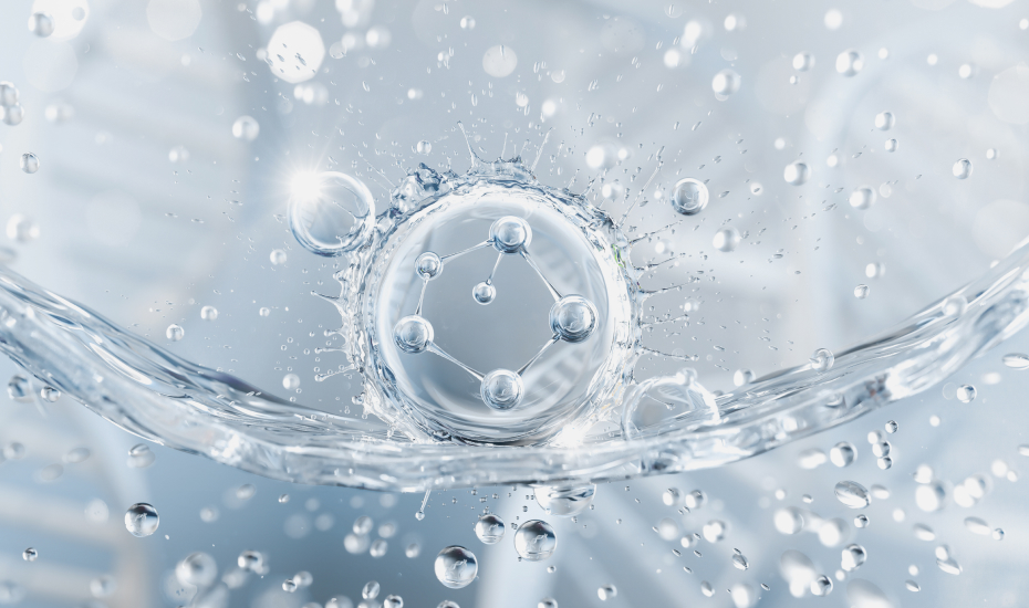
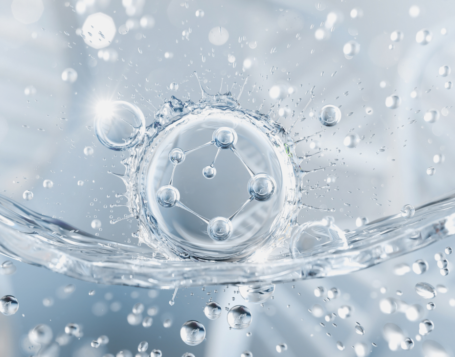
Synthesis of high-performance organic/inorganic materials
Synthesis of high-performance organic/inorganic materials is being researched to develop new products to secure competitiveness in the semiconductor/display business based on existing synthesis technologies. Based on various synthesis technologies, molecular design and additive application technologies, MTI develops and supplies various application products to meet customer requirements.
- Synthesis of various organic/inorganic materials using Sol-Gel method
- Synthesis of various organic and inorganic materials using polyol synthesis
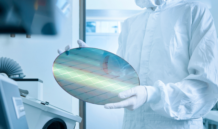
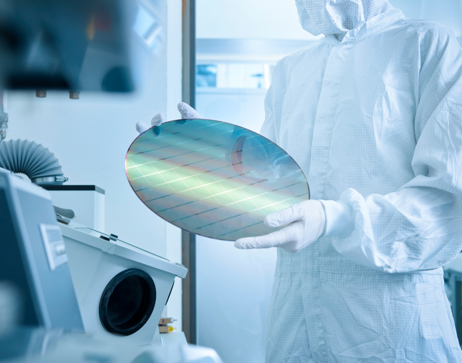
TBDB
Ultra-thin wafers are widely used in high-function devices, but they are very easily damaged, so the existing wafer handling method cannot be used as it is. Also, developing ultra-thin dedicated equipment requires enormous investment. Therefore, in order to use existing equipment as it is, use a wafer or glass as a carrier, complete all processes, separate it from the carrier, and perform the next process. In particular, the advanced packaging field is expected to be the only technological breakthrough as the technology that can improve semiconductor performance by reducing the minimum line width is reaching the physical limit of 30 nm – 20 nm.
Until now, TBDB(Temporary Bonding De-bonding) technology has been developed to handle wafers that are brittle and relatively thick, such as GaN and GaAs, for LED production but TBDB technology for ultra-thin wafers with a thickness of less than 50 μm will be required in the market in the future.


-

mti@mtisemi.com
-

031-493-6737
-

154-23 Wonsi-ro, Danwon-gu,
Ansan-si, Gyeonggi-do
(729 Wonsi-dong)