

-
Company Introduction
-
Business Field
-
Product Introduction
-
Recruitment
-
Community
Film&Tape
MTI ECO INNOVATION
Film&Tape

BG Tape
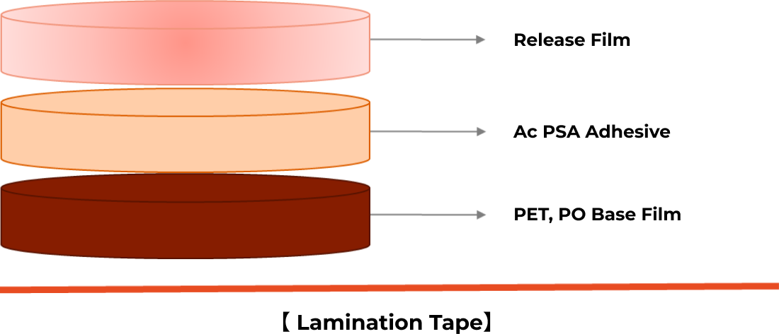
Lamination Tape
This tape is intended to protect the pattern side & bump side of the wafer in the process of grinding the back side of the wafer to the wafer thickness desired by the user.
We have UV PSA and Non PSA Line up by adhesive type.
Description
- Bump, Solder Ball Wafer applied to BG Process
- A structure that can fully dip the solder ball, bump, and pattern side
- High-adhesive UV, Non-UV Adhesive Layer
Applications
- Memory, DDI, COG, AP, CPU, Communication IC, Etc…
Properties
- Adhesion that strongly holds the wafer during the BG process
- Possession of thick adhesive layer suitable for Big Solder Ball
- When removing BG tape after UV curing, peeling is possible without contamination
- Thin Wafer implementation possible
- Very stable tape thickness deviation management
- More reliable TTV guarantee
Product
Structure


-

mti@mtisemi.com
-

031-493-6737
-

154-23 Wonsi-ro, Danwon-gu,
Ansan-si, Gyeonggi-do
(729 Wonsi-dong)